Vellore, India  ·  30+ Years of Experience · Since 1993 info@vitpark.com
Home/Solutions/Semiconductor

An integrated semiconductor ecosystem.

VIT Semicons Park Private Limited, VITPARK's semiconductor company, is setting up an integrated semiconductor ecosystem in Ratnagiri, Maharashtra: from silicon wafers to finished, packaged chips. The Ratnagiri programme is aligned with the India Semiconductor Mission (ISM).

VIT Semicons Park Pvt Ltd · Ratnagiri, Maharashtra
VIT Semicons Park

Leading affordable semiconductor innovation.

We strive to deliver semiconductor products at an affordable cost and the highest quality, to meet the needs of humankind. Our aim is to become a global hub for semiconductor production, reducing import dependence and building skills in India.

From design to manufacturing, we cover advanced chip design, prototyping, testing and scalable production, for modern electronics.

Registered officeNo. 108 & 109, Siddhi Vinayak Complex, Shivaji Nagar, Ratnagiri 415 612, Maharashtra
Admin office13/16, 24th East Cross Road, Gandhinagar, Vellore 632 006, Tamil Nadu
Vision

To bring chip design and manufacturing together in one place, delivering high-performance, energy-efficient products and driving sustainable technological advancement worldwide.

Mission

To deliver efficient, scalable semiconductor manufacturing that power diverse applications and enhance connectivity.

Promise

Delivering quality semiconductors globally, reducing imports and building local capability.
Our business

Three manufacturing stages at one site.

Silicon is grown, patterned and packaged inside the same ecosystem, so quality is controlled from the raw material to the finished device.

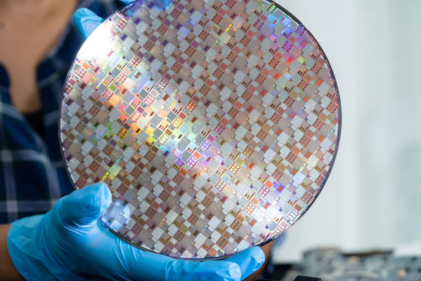
Silicon manufacturing facility

Silicon Wafer Manufacturing

High-purity silicon wafers, sliced with precision and produced to specification for semiconductor applications.

  • High-purity silicon production
  • Precision slicing, uniform thickness
  • Various sizes and specifications
  • Rigorous quality control
Front end

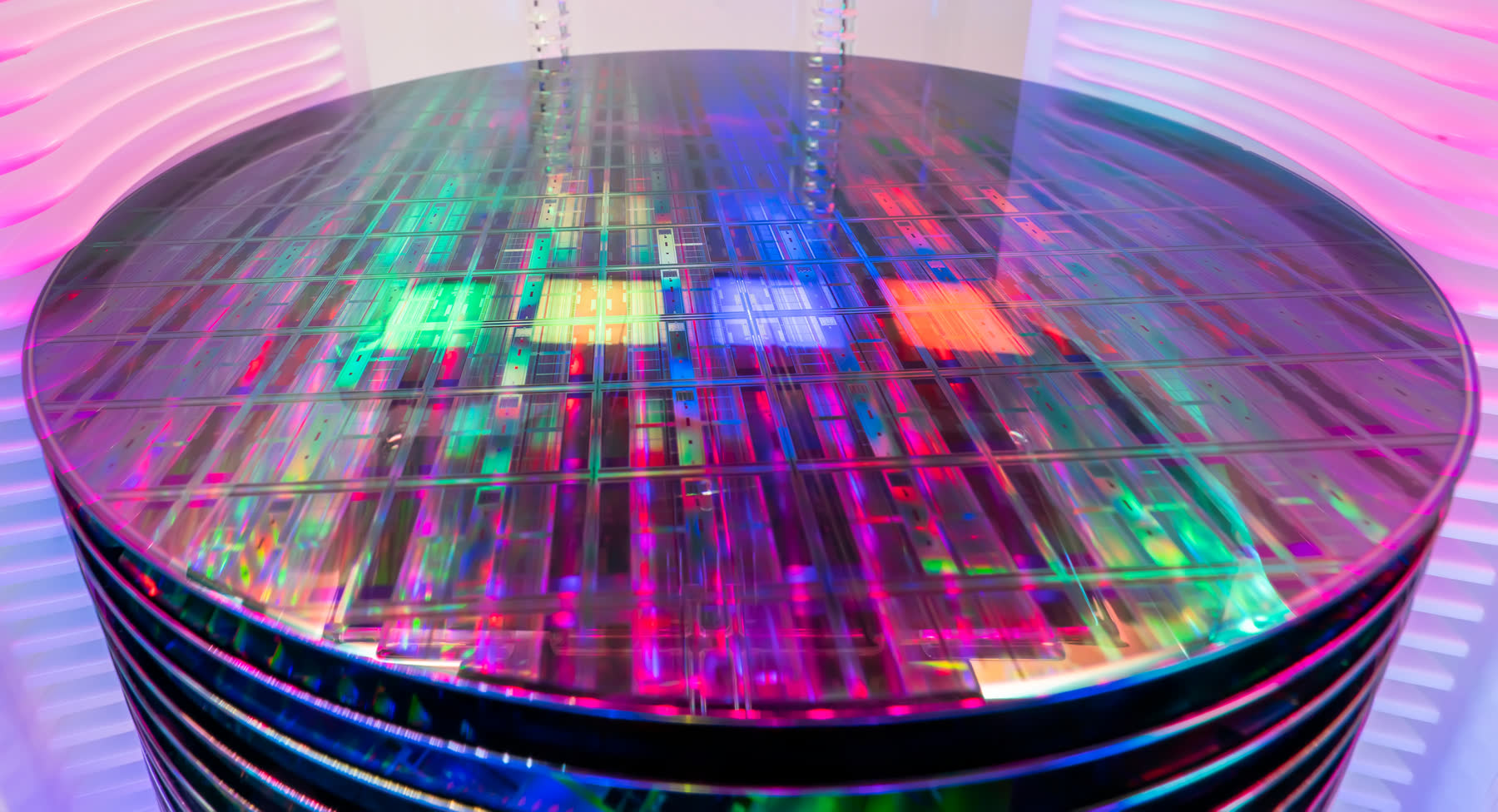
Semiconductor Fabrication Facility

Turning silicon wafers into working devices with advanced lithography, etching and deposition, under stringent quality controls.

  • Lithography, etching and deposition
  • Oxidation and doping processes
  • Cleanroom manufacturing
  • Wafer testing and characterisation
Back end

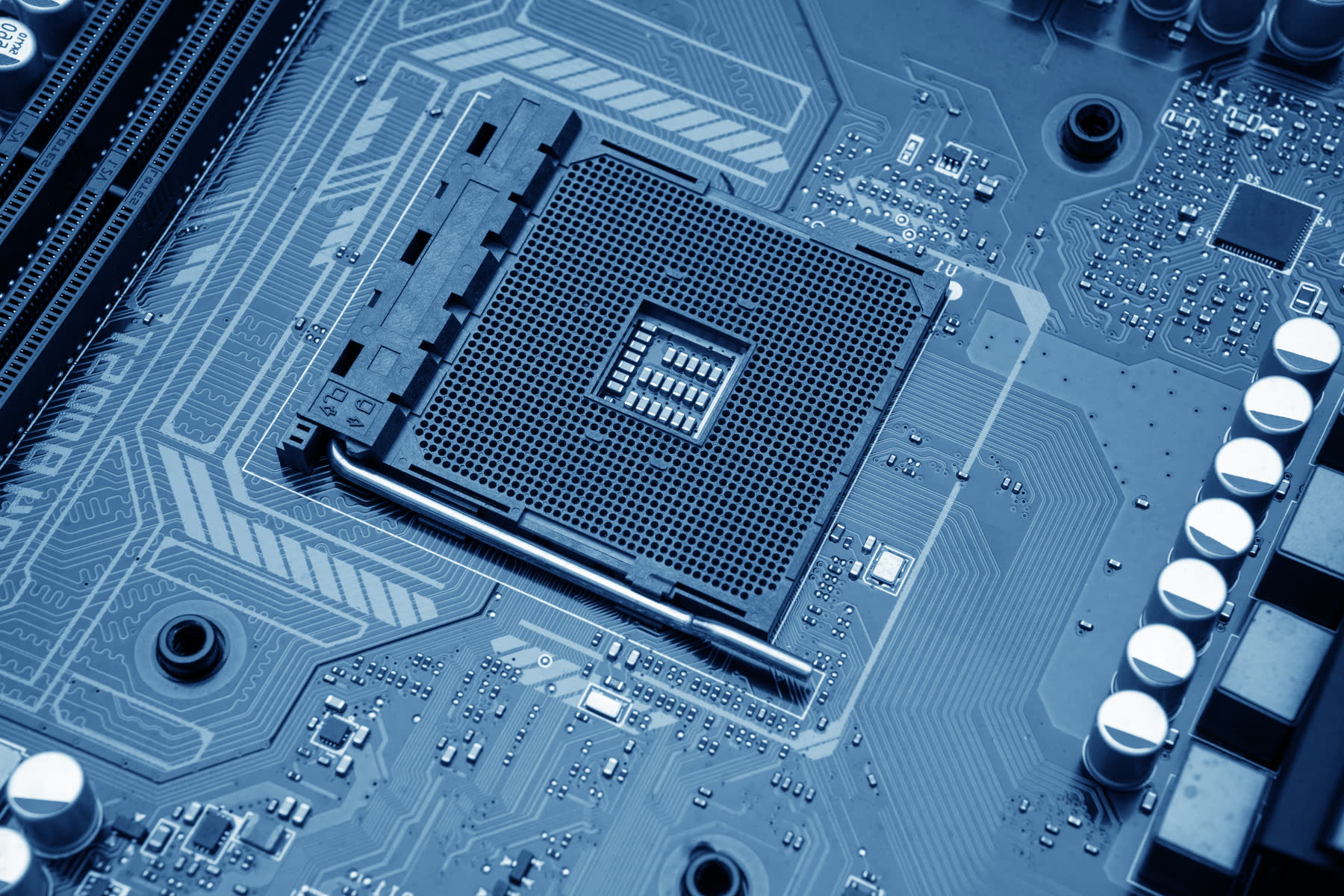
Assembly, Testing, Marking & Packing (ATMP)

The final stages of chip manufacturing: wafer testing, die separation and packaging, so every device is ready for real electronic applications.

  • Die bonding and wire bonding
  • Advanced packaging and encapsulation
  • Rigorous testing and inspection
  • Final inspection and quality assurance
Global technology partners

Backed by the world’s largest semiconductor companies.

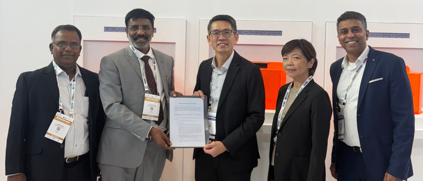
Agreements signed at SEMICON India 2026 in New Delhi, held in the presence of Prime Minister Shri Narendra Modi.

VIT Semicons and KLA leaders with the signed agreement, SEMICON India
Agreement with KLA, SEMICON India 2026, New Delhi.
JP

Hitachi

Hitachi will supply the latest technology and manufacturing machinery for the Ratnagiri project.

Signed by Hiroshi Shimazaki, Executive Officer, Hitachi, and Tajpur Sampath Kannan, Managing Director, VIT Semicons
US

KLA

KLA will provide technical equipment and international-standard, high-tech training for young engineers in Maharashtra.

Signed by Chia Wee Tech, Executive Officer, KLA, and Tajpur Sampath Kannan, Managing Director, VIT Semicons

Fabless and manufacturing

VIT Semicons is a semiconductor company in the fabless and manufacturing sectors. At Watad and Jadgaon MIDC, Ratnagiri, it is building a semiconductor park to design and manufacture advanced chips for silicon wafers, mobiles, automobiles and data centres, reducing India’s dependence on imports.

Integrated semiconductor project

From silicon to finished chips.

India is building its own chip supply chain. VITPARK's integrated semiconductor project covers the full manufacturing path, using established fabrication processes and modern design methods.

  1. Silicon extraction

    Quartzite refined to electronic-grade silicon via the Siemens process.

  2. Wafer production

    Purified silicon processed and sliced into precision wafers.

  3. Photolithography

    Wafers coated with photoresist, exposed and developed to reveal patterns.

  4. Etching & doping

    Patterns etched and doped to set electrical properties.

  5. Metallization

    Metal layers added for the connections that form circuits.

  6. Assembly & test

    Chips assembled, tested, marked and packed.

Looking for a manufacturing, technology or investment partnership in semiconductors? Our programme team will take you through the roadmap.

Discuss a partnership
More from VITPARK

Explore our other solutions.

Related solutions.

Talk to our team.

Have a technology challenge or a new idea? Tell us what you need, and the right VITPARK team will get back to you within one business day.

Version 6